01 / Atomistic Simulation
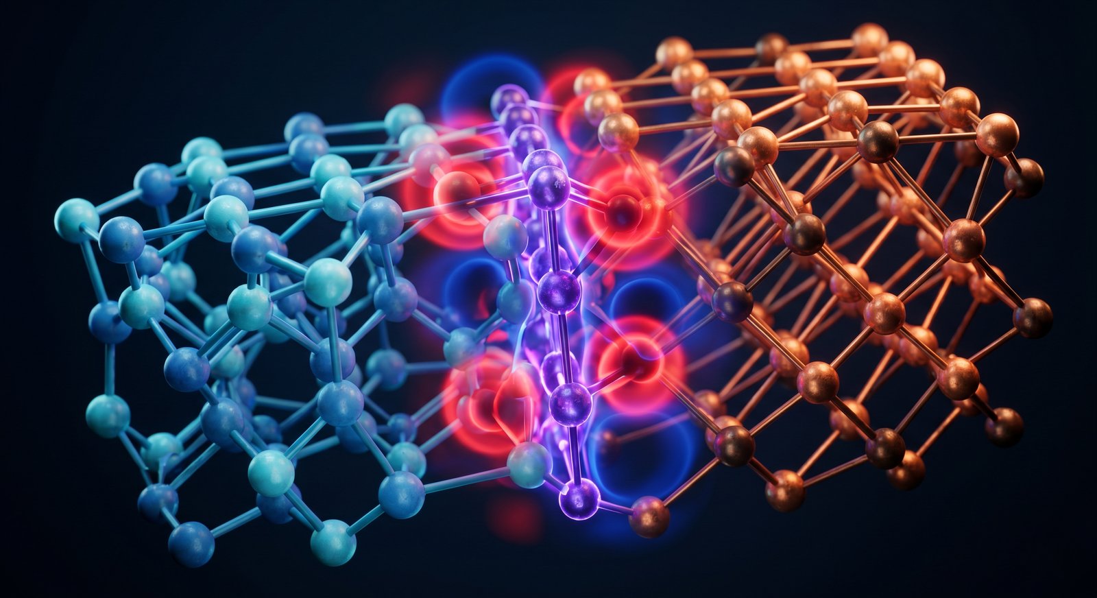
Atomistic simulation of solid-state bonding 固相接合の原子レベルシミュレーション
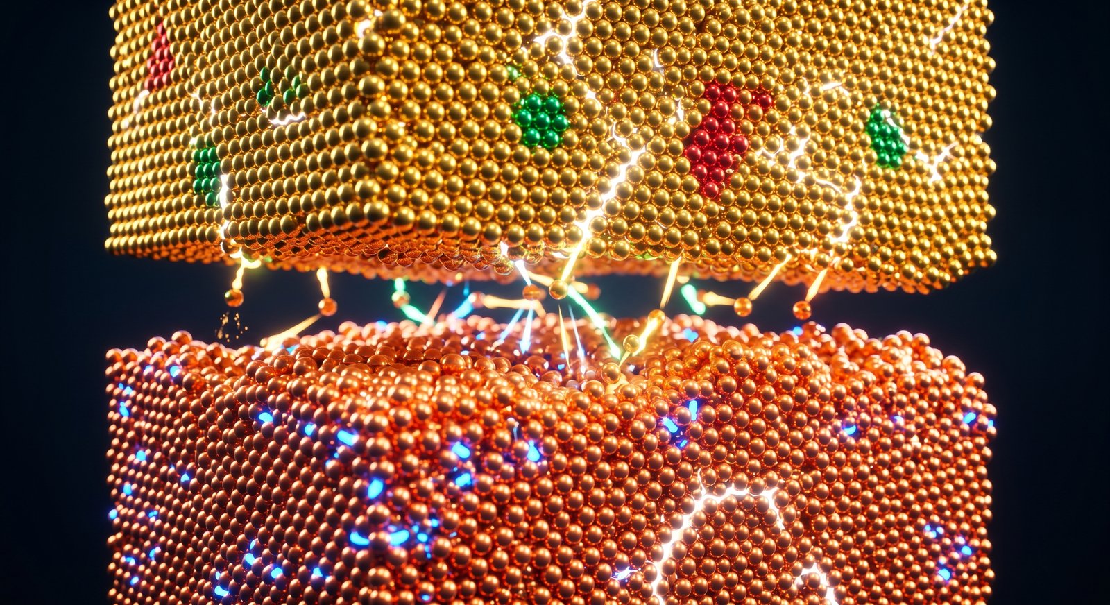
Cu-to-Cu solid-state bonding is a key enabler of 3D semiconductor packaging, but its underlying atomistic mechanisms — surface nanostructures, grain boundaries, and crystallographic orientation effects — remain poorly understood at the continuum level. Using molecular dynamics on supercomputers including Fugaku, we resolve how atoms reorganize during bonding and translate those insights into design rules for real interfaces. Cu–Cu 固相接合は三次元半導体実装を支える基盤技術でありながら、その背景にある原子レベルの機構 — 表面ナノ構造、結晶粒界、結晶方位 — はマクロな解析からは見えにくい領域です。富岳をはじめとするスーパーコンピューターを用いた分子動力学シミュレーションにより、接合中の原子再配列を分解し、その知見を実材料の界面設計指針に橋渡しすることを目指しています。
Molecular dynamics
Cu–Cu bonding
Twin boundaries
Surface nanostructures
3D packaging
Fugaku
Selected papers (lead author)主要論文 (主著・責任著者)
Atomistic behavior of Cu–Cu solid-state bonding in polycrystalline Cu with high-density boundaries
Impact of crystalline orientation on Cu–Cu solid-state bonding behavior by molecular dynamics simulations
Solid-state bonding behavior between surface-nanostructured Cu and Au — a molecular dynamics simulation
 Atomistic Simulation